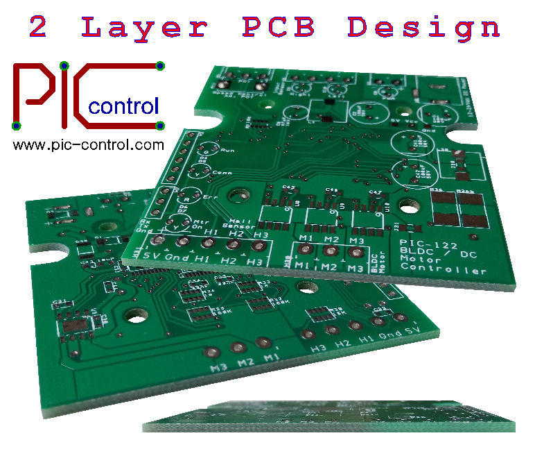
Our speciality is focusing on mostly on 2 layers (double layer) or single layer PCB board design. Laying out a 2 layer PCB board is more challenging and takes much more time compared to a multi-layer PCB board design. There is much less space for the trace routing. Components placement has to be strategically planned to ensure shorter traces. Components have to be studied and group closely together depending on the circuit design.
We have strict design practice to help keep the circuit signal integrity tight, to reduce the possibility of noise generated from the trace route. This is also the reason why we do not use automated-routing provided by the PCB CAD software. Our PCB layout is done manually, components neatly laid and trace routed with signal integrity in mind. So your next question might be, why 2 layers PCB board? Why the extra effort for a 2 layer PCB design?
Why 2 Layer PCB board?
The main reason for designing a 2 layer PCB board and spending the extra effort to route is to reduce the cost of production and maintenance. Cost is everything especially when your production volume is high. Every cent makes a difference, every cent count. Click here for a PCB specification of a typical 2 layer PCB board.
Reduce Production Cost
Most electronic designs that are not limited by any space constraint typically uses 2 layer board. The cost of producing a 2 layer PCB board cost less than a multi-layer board. If each board cost a dollar less to produce, it means that the more circuit boards you produce, the more you will save by using a 2 layer board instead of a multi-layered board. The initial design cost may be higher, but in long run, our customers will save more. Whenever possible, we will always want to recommend to a customer to fit their design onto a 2 layer PCB board.
Reduce Maintenance Cost
In terms of maintenance, 2 layer board is simpler too. The board is easier to work with, easier to troubleshoot. Modification or repair work is possible since the trace is on either side of the PCB board. Multi-layer PCB boards have hidden layer which is not easily access. Troubleshooting can be difficult especially the trace in the inner layer is not fabricated properly. Replacement of faulty components may also damage the internal layer of a multi-layered board, which can only be examined through X-Ray. Problem detected on a multi-layer board would usually mean a new replacement. All these hidden costs can make your circuit board product more expensive to maintain.
We highly recommend constraining your design to a 2 layer PCB board.
We love designing 2 layer PCB.
PIC-CONTROL has the experience and expertise to optimise your PCB circuit design for maximum production efficiency. We design a reliable product with production and maintenance cost in mind.
Contact our Sales Engineer for consultation,
to assist you with the right solution.
Contact PIC-CONTROL today!

